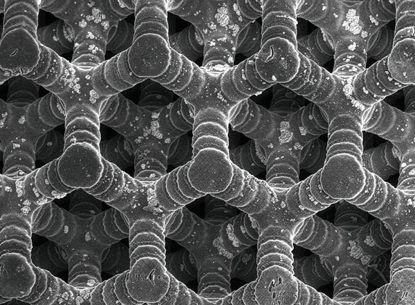
Tabletop 3D Printing Cuts Semiconductor Patterning From Days to Minutes
Tabletop 3D Printing Meets Semiconductor Manufacturing
The semiconductor industry has long been dominated by a handful of companies with the resources to afford Extreme Ultraviolet (EUV) lithography machines — devices that cost upwards of $200 million and occupy entire rooms. But a breakthrough from the University of Texas at Austin is changing the equation. Researchers in the Cockrell School of Engineering have developed a tabletop EUV lithography device paired with a novel 3D printing technique that cuts semiconductor nanopatterning from days to just minutes.
The research, published in Nano Letters, introduces volumetric 3D patterning — a method that prints multiple layers of 3D nanostructures simultaneously rather than the traditional layer-by-layer approach. “The actual printing might not take very long,” said Professor Chih-Hao Chang, one of the lead authors. “But the processing can take days.” With the new technique, exposures take minutes instead.
Why This Matters for 3D Printing
While this technology is still years away from commercial semiconductor production, it represents a fascinating convergence of 3D printing principles and advanced manufacturing. The core idea — using parallel printing to create complex 3D structures in a single pass — echoes what the consumer 3D printing revolution has been about: making complex manufacturing accessible, faster, and cheaper.
The tabletop device strips traditional EUV lithography down to its essential components, making it modular and affordable enough for university labs. Currently, the process can pattern periodic structures useful in memory chips and photonics. The ultimate goal is to create even smaller switches inside semiconductors, giving each chip more computing power.
Beyond Semiconductors: Cross-Industry Applications
The implications extend far beyond computer chips. As lead author Saurav Mohanty noted, “Beyond semiconductor manufacturing, the ability to pattern 3D nanostructures can find applications in medicine for nanodrugs, quantum computing, or synthesizing novel materials.” This kind of cross-pollination between 3D printing techniques and other industries is exactly where the most exciting innovations emerge.
The research stems from the National Science Foundation Future of Semiconductors (FuSe2) competition, which focuses on driving down the cost of semiconductor research. By making EUV lithography accessible to more researchers, the team hopes to accelerate innovation across the entire semiconductor ecosystem.
How TT3DPrint Can Help
At TT3DPrint, we understand the power of making advanced manufacturing accessible. While we work at the macro scale with FDM printing rather than the nanoscale, our mission aligns with this research: delivering high-quality, custom 3D printed parts quickly and affordably. Whether you need prototypes, functional parts, or custom figurines, our Bambu Lab printer cluster ensures fast turnaround and consistent quality.
Ready to bring your designs to life? Contact us today for a free quote on your next 3D printing project.
Conclusion
The convergence of 3D printing and semiconductor manufacturing represents one of the most promising frontiers in advanced manufacturing. As tabletop devices make EUV lithography more accessible, we can expect a wave of innovation in nanoscale 3D printing — from faster chip production to new medical applications. The future of manufacturing is getting smaller, faster, and more accessible.
Source: University of Texas at Austin, “Three-Dimensional Nanopatterning Using Extreme Ultraviolet Colloidal Talbot Lithography,” Nano Letters (2026). DOI: 10.1021/acs.nanolett.6c01662